

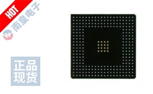
Production Overview
оƬ��ُ�W��ע���χ������ڙ�IC�����̵ĬF؛�YԴ�����r��ԃоƬ��棬�����ИI�r���p�ɲ�ُICоƬ���LJ��Ȍ��I��оƬ��ُƽ�_��
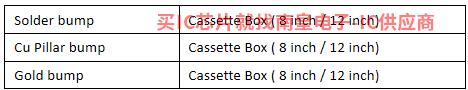
TFME is able to provide Solder bump, Cu pillar bump and Gold bump for customer to meet different requirement.
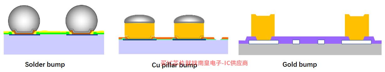
Solder bump Cu pillar bump Gold bump
- Wafer size: 8 inch / 12 inch - Wafer size: 8 inch / 12 inch - Wafer size: 8 inch / 12 inch
- Structure: 0P1M~2P2M - Structure: 0P1M~1P2M -Structure: 0P1M~1P1M
- Body size: 0.7*0.76~10.7*10.7 mm - Body size: 1.0*1.5~10*10mm - Structure: 0P1M~1P1M
- RDL L/S: min.5um/5um - RDL L/S: min. 5um/5um - Bump L/S: min.10um/8um
Solder bump & Cu pillar
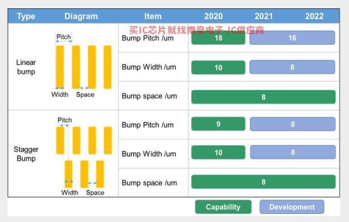
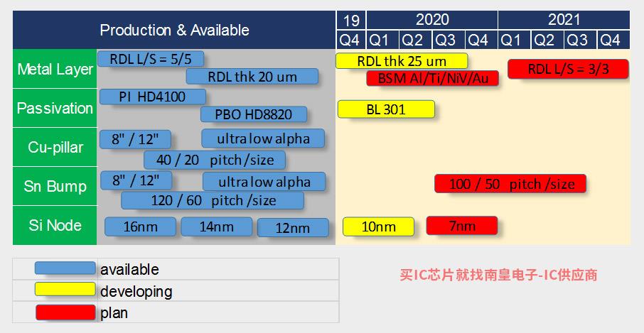
Process Capability & Design Rule
Gold bump
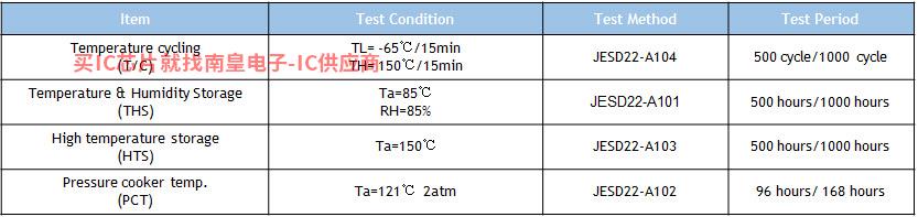
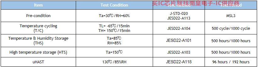
Reliability Test Standards
Solder bump & Cu Pillar bump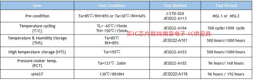
Gold bump
Shipment Packing
Production Overview
TFME offers various Wafer Level CSP product to customer including Fan in type and Fan out type.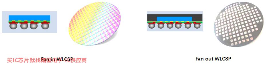
Feature
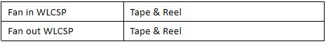
Fan in WLCSP Fan out WLCSP
- Ball count : 2~309 - Ball count : 36 ~203
- Structure: 1P1M~2P2M - Structure: 1P1M~3P3M
- Body size: 0.6*0.3~7.6*7.6mm - Body size: max 20*20mm
- RDL L/S: min.5um/5um - RDL L/S: min.2um/2um
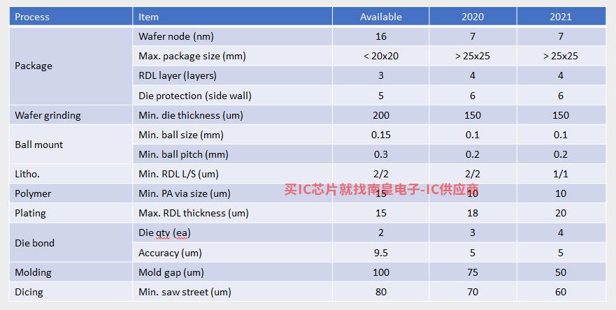
Process Capability & Design Rule
Fan in WLCSP
Process Capability & Design Rule
Fan out WLCSP
Reliability Test Standards

Shipment Packing
Production Overview
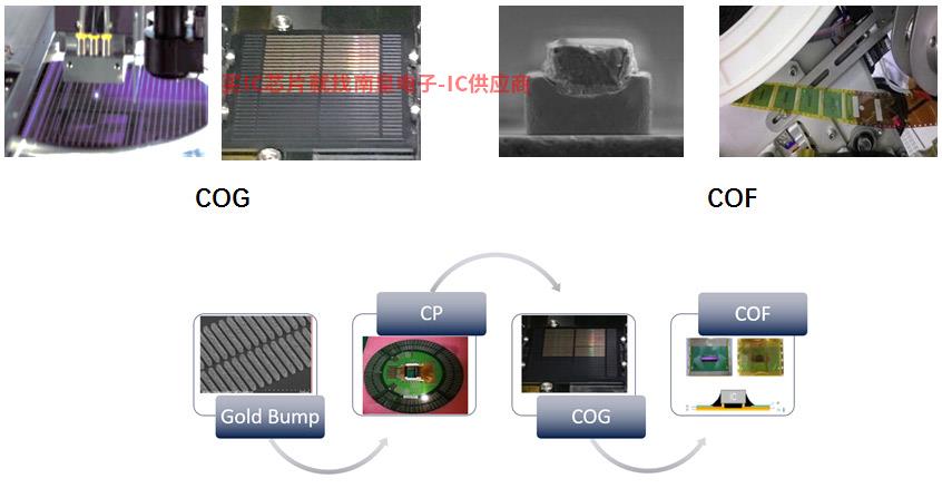
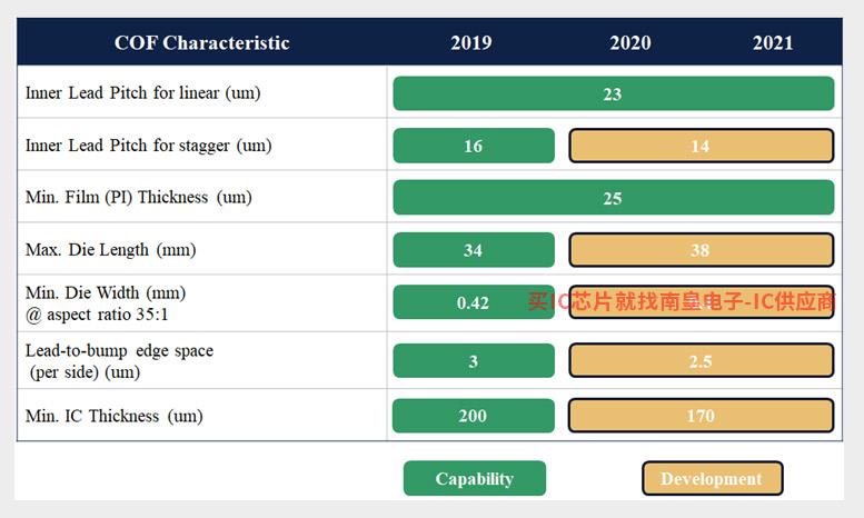
TFME is able to provide COG (Chip On Glass) and COF (Chip On Film) services for gold bump drive ICbased on customer requirement.
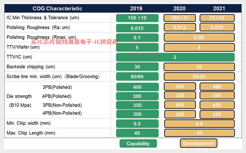
Process Capability & Design Rule
COG
Process Capability & Design Rule
COF
Reliability Test Standards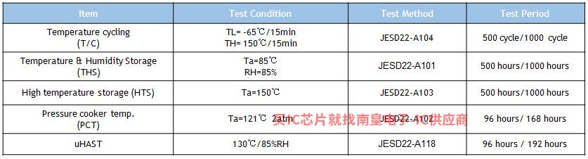
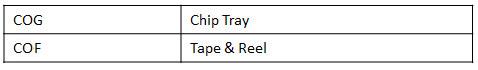
Shipment Packing
Production Overview
Flip Chip interconnection, also knownas Controlled Collapse Chip Connection, C4, has been identified as a high performance packaging solution to meet the growing need for products with increased electrical performance, high I/O, and high system reliability as a replacement for conventional wire bond process. Utilizing whole die area as for electrical connection, substrate I/O per unit exponentially increased vs. perimeter wire interconnection technology.
Flip chip interconnect also allows direct connection with on-die power planes which enables increased electrical performance including increased switching speed and more efficient power distribution to the IC performance at lower operating voltages.
TF-AMD Flip Chip are assembled with single unit laminate which is the highest routing density through build-up technology to maximize the device performance &conventional ceramic substrate for reliability enhanced package solution. Combined with Flip Chip interconnection, TF-AMD provides optimal design flexibility for final package design& product format to fit an end user requirement.TF-AMD offers Flip Chip BGA packages with ball counts up to 3000 & PGA package up to 2000
Application
Flip Chippackage is considered one of the most established industry platform applicable for high pincount and/or high performance ASICs. Large body FC BGA/PGAs provide package solution forComputing (microprocessors / graphic, server), gaming,high bandwidth networking/Communicationdevices. Combined with Flip Chip technology &BGA/PGAlead format, TF-AMD help to enable SMT and also pin insertion application.
Features
Flip Chip BGA/PGA Packaging
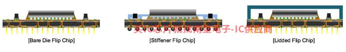
Package Types: Bare die, Stiffener, Lidded (Top hat & flat top)
Wafer Node 314/16nm ELK(extreme low K) qualified, 7nm in development.
Package sizes from 12mm to 55mm (75mm in development)
Die area up to 800mm^2
Lead Free, Eutectic, High-Pb bump for Flip Chip connection
Passive component size down to 01005
High thermal performance solution using Indium metal TIM
Substrate
o 4 �C 18 layers laminate build up
o Coreless, 0.2mm, 0.4mm, 0.8mm, 1.0mm available
o High CTE ceramic / LTCC alumina ceramic
o BGA / PGA
Footprints Pitch
o BGA : 0.5mm, 0.65mm, 0.8mm and 1.0mm
o PGA : 1.0mm, 1.27mm
Other Option
o Multi-die capability
o Die binning to waffle pack up to 256 BINs
Flip Chip BGA/PGA Test
Test Product Engineering
o TF-AMD test provides a competitive test solution to our customers ranging from test development, platform conversion, and product maintenance and test data analysis.
o The team has rich test development experience of various product portfolio, including high-end digital, mix-signal, SOC and high speed products.
Adding Value to Customer
o Reduce customer overhead by outsourcing projects / tasks to avoid maintaining a large scale of dedicated team
o Incorporate industrial standard through leveraging best known method from our database & continuous cost saving by driving test time reduction, yield improvement
Service Solutions
o Wafer Sort test development
o Final Test development
o Low cost platform conversion
o Multi-site enablement
o Burn-in capabilities
Test Development Experience
o CPU, APU, GPU
JST���� o Chipset
o Digital Audio
o Baseband
o Microcontroller
o LCD Driver
o Touch Panel Driver
ATE platforms and products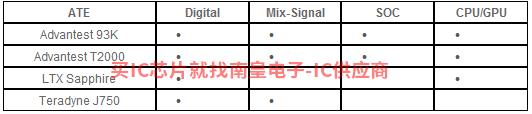
Reliability Test Standards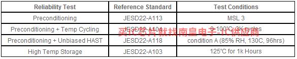
Design Rule
Top Hat Single Piece Lid
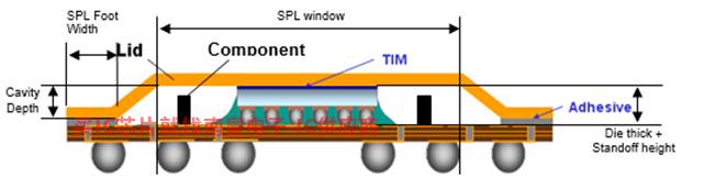
Lid size=substrate size-0.2mm
Standard foot sizes
o 2mm for 15-25mm body
o 3mm for 27-31mm body
o 4mm for 33-50mm body
Max 3mm on all four sides (UF will flow under the bend/slant of the HS). Extended design rule allow Max. 2.5mm for the body size ��31mm
Lid is centered
Cavity depth for 12inch wafer SPL is 0.8mm and total thickness is 1.3mm
o TIM Thickness target: 40um (Max. 100um)
o Adhesive Thickness target: 120um (Max. 200um)
o Lid manufacturing tolerance: +/-50um
Body size<31mm support bare die structure (without stiffener/lid construction)
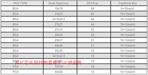
Packing & Shipping (in house standard)
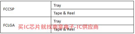
BGA / PGA (Tray)
Production Overview
TFME offers various FCCSP and FCLGA package based on customer different requirement.
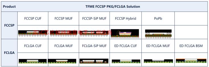
Features
- SiP (FC + SMT + Wire bond) available.
- CUF, MUF available.
- 7N/12N/14N/16N wafer node mass production
- Various substrate technology qualified including SAP, MSAP, ETS, MIS and SLP.
- Fully Turnkey for wafer bumping, probing, assembly, FT available.
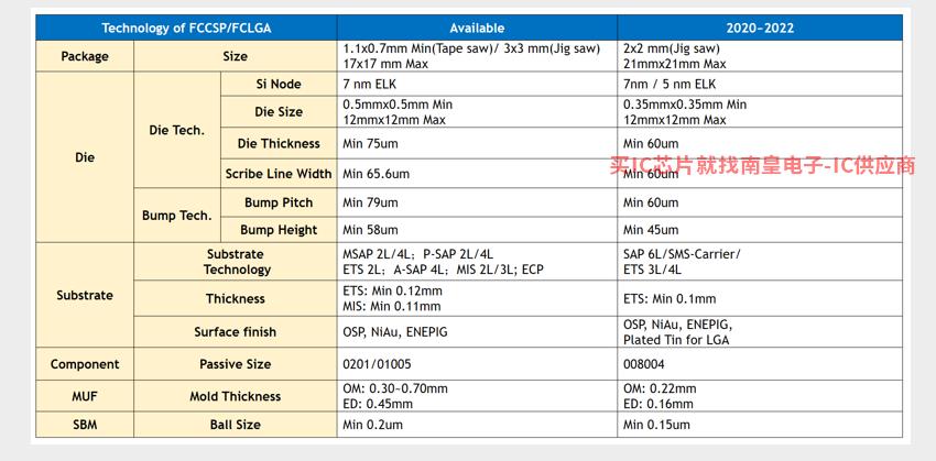
ProcessCapability & Design Rule
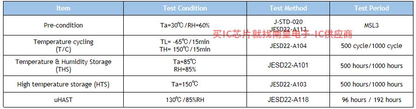
Reliability Test Standards
Shipment Packing
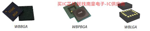
Production Overview
TFME offers various WBBGA and WBLGA package based on customer different requirement.
Features
- 1.1x0.7 mm to 21x21 mm Package
- 0.2mm to 1.0mm C Mold Chase
- 01005 Components SMT
- 0.3x0.3 mm Small Die
- 1-6 Layer Substrate
Process Capability & Design Rule
Reliability Test Standards
Shipment Packing


- SpaceX�����^17�|��Ԫ�����Y ��ֵ���ӵ�1270�|��Ԫ
- e�N�ۖ|֥���µ����ܖŘO����
- RISC-V�I����ِ���Ƽ��Ї�IC���ǫF�Q̖
- ɳ�ذ�����Ӌ�����_ 2026 ����ڳ� 15 �f�v늄���܇
- AI����оƬ���ĵø��ã��ĵø��ã� �����pӰ���|��ŞAlpha 7R V�l��
- Ӣ�ؠ����Z2040�� ÿ�ꌍ�F���Қ��w�����ŷ�
- IAR Systems ȫ��֧�� Renesas RH850��������܇�ИI�Ą���
- AVEVA���Sܛ���@�Ã���������쪄�
- �K�ڵȺ��ײ��ˣ��l��1050 5G̎�����l��
- �ɂ�������������룬�@������FPGA�Ƽ���˾ҪѸ������
- LG ����Դ���鸣���ṩ�������܇늳أ��s�ό��r��
- ��2030�꣬���й��S��75%��������Կ�������Դ
